|
|
|
|
Indium Tin oxide (In2O3-SnO2) ITO sputtering target CAS 50926-11-9
Model No.︰
ITO
Brand Name︰
TYR
Country of Origin︰
China
Unit Price︰
US $ 200 / pc
Minimum Order︰
1 pc
Product Description
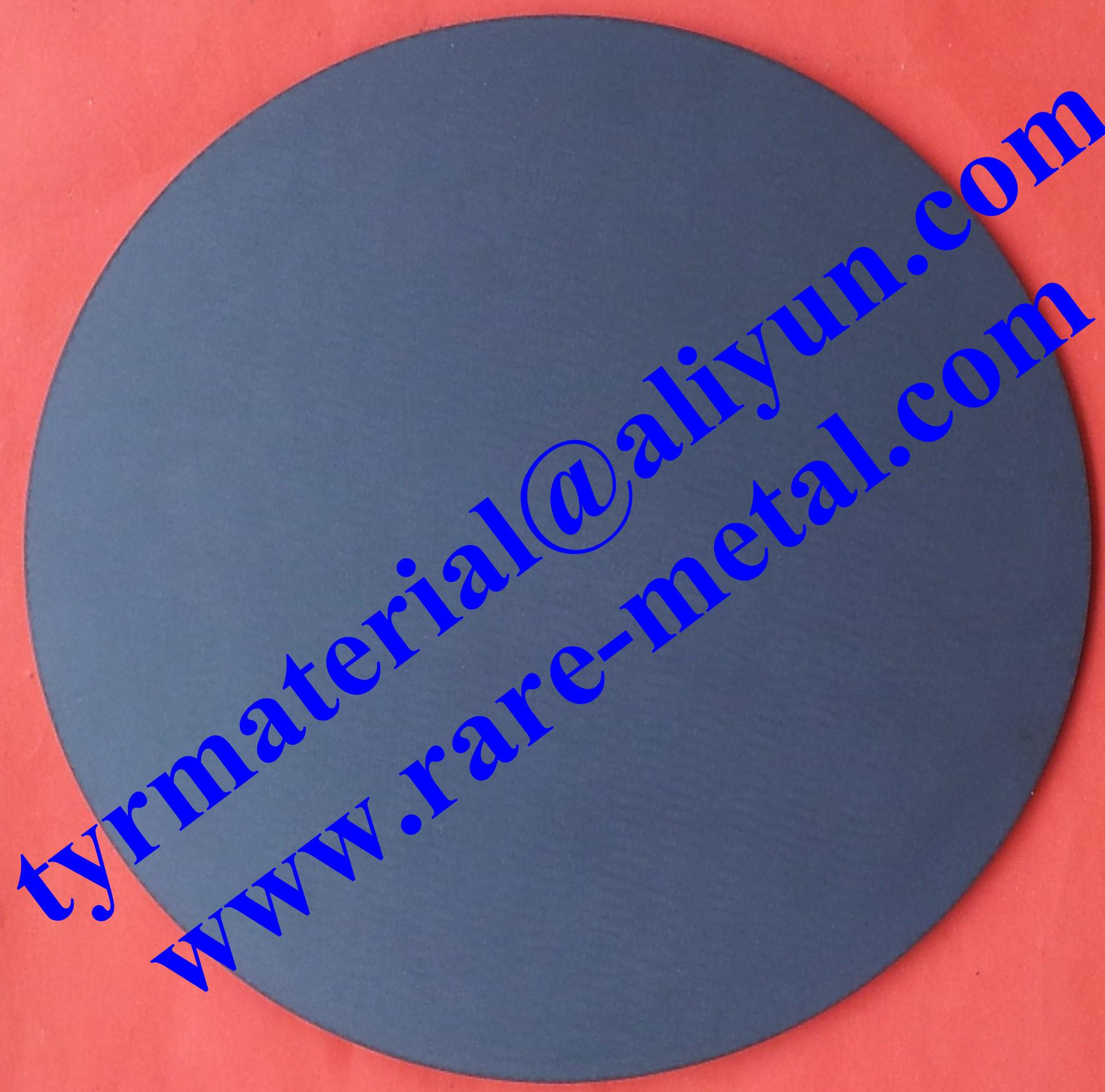
Indium Tin oxide (In2O3-SnO2) ITO sputtering targets
Purity: 99.99%
composition: Per requested from customer
In2O3/SnO2=90/10wt
In2O3/SnO2=50/50wt,
In2O3/SnO2=60/40wt
Diameter: 355.6mm (14") max.
Single piece Size: Length: <500mm, Width: <250mm, Thickness: >1mm, if larger size than this, we can do it as Tiles joint by 45 degree or 90 degree
Shape: Discs, disks, step disk, delta, plate, sheets or made per drawing
Density: RD>99%
Made sputtering targets method: hot pressing (HP), hot/cold isostatic pressing (HIP, CIP), and vacuum melting, vacuum sintering
Indium tin oxide (ITO, or tin-doped indium oxide) is a solid solution of indium(III) oxide (In2O3) and tin(IV) oxide (SnO2), typically 90% In2O3, 10% SnO2 by weight. Its melting point is 1526-1926 oC , Density, 7.120–7.160 g/cm3, Color (in powder form): Pale yellow to greenish yellow,
depending on SnO2 concentration
It is transparent and colorless in thin layers while in bulk form it is yellowish to grey. In the infrared
region of the spectrum it acts as a metal-like mirror.
Indium tin oxide is one of the most widely used transparent conducting oxides because of its two chief
properties, its electrical conductivity and optical transparency, as well as the ease with which it can be
deposited as a thin film. As with all transparent conducting films, a compromise must be made between
conductivity and transparency, since increasing the thickness and increasing the concentration of charge
carriers will increase the material's conductivity, but decrease its transparency.
Thin films of indium tin oxide are most commonly deposited on surfaces by physical vapor deposition.
Often used is electron beam evaporation, or a range of sputter deposition techniques.
Applications:
ITO is often used to make transparent conductive coatings for displays such as liquid crystal displays, flat
panel displays, plasma displays, touch panels, and electronic ink applications. Thin films of ITO are also
used in organic light emitting diodes, solar cells, antistatic coatings and EMI shieldings. In organic
light-emitting diodes, ITO is used as the anode (hole injection layer).
ITO films deposited on windshields are used for defrosting aircraft windshields. The heat is generated by
applying a voltage on the film.
Thin film interference caused by ITO defrosting coating on an Airbus cockpit window. The film thickness
is non-uniform on purpose, preventing uneven removal of ice/frost.
ITO is also used for various optical coatings, most notably infrared-reflecting coatings (hot mirrors) for automotive, and sodium vapor lamp glasses. Other uses include gas
sensors, antireflection coatings, electro wetting on dielectrics, and Bragg reflectors for VCSEL lasers.
ITO was also used as a sensor coating in the later Kodak DCS cameras, starting with the Kodak DCS 520,
as a means of increasing blue channel response.
ITO thin film strain gauges can operate at temperatures up to 1400 °C and can be used in harsh
environments, e.g. gas turbines, jet engines, and rocket engines.
The primary advantage of ITO compared to AZO as a transparent conductor for LCDs is that ITO can be
precisely etched into fine patterns. AZO cannot be etched as precisely: It is so sensitive to acid that it
tends to get over-etched by an acid treatment.
Another benefit of ITO compared to AZO is that if moisture does penetrate,TO will degrade less than
AZO.
composition: Per requested from customer
In2O3/SnO2=90/10wt
In2O3/SnO2=50/50wt,
In2O3/SnO2=60/40wt
Diameter: 355.6mm (14") max.
Single piece Size: Length: <500mm, Width: <250mm, Thickness: >1mm, if larger size than this, we can do it as Tiles joint by 45 degree or 90 degree
Shape: Discs, disks, step disk, delta, plate, sheets or made per drawing


